Carrito de compra
Su pedido cuenta con 0 productos
Envío gratis a partir de $389.00 (Consulta T&C)
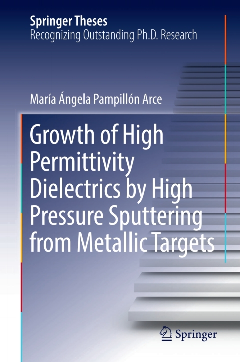
| ISBN: | 9783319666075 |
|---|---|
| Formato: | Page Fidelity |
| Idioma: | Inglés |
| Editorial: | Springer Nature |
| Tema: | Ciencia |
| Subtema: | Física materia condensada |
| Año de publicación: | 2017-10-04 |
This thesis describes the fabrication of metal-insulator-semiconductor (MIS) structures using very high permittivity dielectrics (based on rare earths) grown by high-pressure sputtering from metallic targets. It demonstrates the possibility of depositing high permittivity materials (GdScO3) by means of high pressure sputtering from metallic targets using in situ plasma oxidation on Si and indium phosphate (InP) substrates. The advantage of this system is the high working pressure, which causes the particles to undergo multiple collisions and become thermalized before reaching the substrate in a pure diffusion process, thus protecting the semiconductor surface from damage. This work presents a unique fabrication using metallic targets and involving a two-step deposition process: a thin metallic film is sputtered in an Ar atmosphere and this film is then plasma oxidized in situ. It also demonstrates the fabrication of GdScO3 on Si with a permittivity value above 30 from metallic Gd and Sc targets. Since co-sputtering was not possible, a nanolaminate of these materials was deposited and annealed. The electrical properties of these devices show that the material is highly interesting from a microelectronic integration standpoint.







 Este sitio web utiliza cookies para mejorar la experiencia del usuario y asegurar su funcionamiento con eficacia.
Al utilizarlo usted acepta el uso de cookies.
Este sitio web utiliza cookies para mejorar la experiencia del usuario y asegurar su funcionamiento con eficacia.
Al utilizarlo usted acepta el uso de cookies.